Alternative Silicon-on-Insulator (A-SOI) wafers
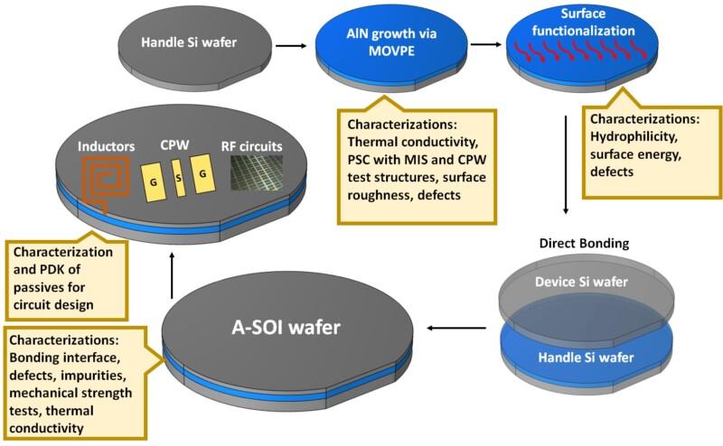
The rapid advancements in 5G, 6G, and beyond present fundamental challenges, particularly increased power consumption and self-heating in RF front-end (RFFE) modules, impacting performance and reliability. Future mobile communications demand more complex and functional RFFE modules, making thermal management crucial. The Electronics Integration and Reliability (EILB) group is focussing on addressing these challenges at the wafer substrate level. We are developing Alternative Silicon-on-Insulator (A-SOI) wafers using aluminium nitride (AlN) with high thermal conductivity (≈ 318 W/m·K) as a buried insulator for enhanced heat dissipation to overcome the self-heating of devices and circuits.
We are using metalorganic vapor-phase epitaxy (MOVPE) reactors to grow AlN with high crystalline quality and high thermal conductivity, refining direct bonding process and surface treatments to create high quality A-SOI wafers. The outcome will be evaluated by manufacturing commonly employed RF passives on A-SOI wafers, developing process design kits (PDKs) to bridge the gap between materials, fabrication, and circuit design, which would ultimately enable RF analog circuit design on A-SOI wafers.