Defect engineering

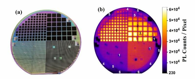
Defects and impurities (e.g. oxygen, metals, dislocations, point defects) are most often harmful when present in semiconductor devices. With deep understanding of relevant defect reactions and gettering mechanisms, it is possible to tolerate the defects without affecting the device performance. Our studies include gettering e.g. by P/B diffusion, SiOx precipitates, Al layer, implantation. The applications can be either high purity semiconductors or solar grade / upgraded metallurgical semiconductors. Our research activities include also the development of characterization methods for defects, e.g. based on minority carrier lifetime.
